



Stack Semiconductor

Explore Our Comprehensive Services: Stack Semi EDA Provider, Expert Training, and Specialized Consultancy

At Stack Semi, we pride ourselves on being a leading provider of  Chinese Electronic Design Automation (EDA) solutions tailored for the semiconductor industry. Our offerings extend beyond just tools—we also provide in-depth training programs designed to equip professionals with the knowledge and skills they need to excel in their roles. Additionally, our specialized consultancy services are available to help businesses optimize their design processes, innovate effectively, and navigate the complexities of the ever-evolving semiconductor landscape. Whether you're looking to enhance your team’s expertise or seeking strategic advice, Stack Semi is here to support your success every step of the way.

Element 2
Element 2

Our Team

Dr Kamarulzaman bin Mohamed Zin, former CEO Silterra,  is a highly accomplished professional who currently serves as the Chief Executive Officer. With a rich and extensive background in the industry, he brings a wealth of knowledge and expertise to his role.


Ken Khoo, co-founder, a seasoned Silicon Valley industry veteran with an impressive career spanning 30 years, adds a significant depth of experience to the team. His long-standing commitment and dedication to the field have greatly contributed to the success and growth of the organization.

Our Philosophy

Foster innovation and provide robust support for Malaysian foundries and their surrounding ecosystem. Our commitment aims to enhance the capabilities of local foundries, promoting advancements that drive growth and sustainability within the industry while ensuring a thriving environment for all stakeholders involved.
Element 2

Stack Semiconductor

Understanding China’s Semiconductor EDA Ecosystem

Stack Semiconductor helps engineers, universities, and semiconductor organizations understand and navigate China’s rapidly evolving Electronic Design Automation (EDA) ecosystem.

Our focus is on the three foundational layers shaping the modern Chinese semiconductor design stack:

  • Full-flow IC Design Platforms
  • Device Physics and Silicon Modeling
  • Verification, Emulation, and AI-Assisted Validation

As global semiconductor development accelerates, understanding the structure of China’s EDA ecosystem has become increasingly important for ASEAN semiconductor ecosystems, universities, IC design teams, and advanced semiconductor research initiatives.


The Three Pillars of China’s EDA Ecosystem

1. The Chinese EDA Ecosystem

China’s semiconductor EDA ecosystem is structured differently from traditional Western EDA models.

Instead of relying on a single dominant platform provider, China has developed multiple specialized EDA companies that focus on different layers of the semiconductor design flow.

This structure allows specialization across:

  • IC implementation and physical design
  • Device modeling and silicon behavior simulation
  • Verification, emulation, and AI-assisted design validation

The modern China EDA stack is increasingly centered around three major ecosystem pillars:

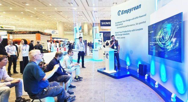
Empyrean Technology

A full-flow semiconductor EDA platform focused on:

  • Digital IC design
  • Analog and mixed-signal design
  • Physical design implementation
  • Manufacturing-aware EDA workflows
  • IC layout and signoff flows

Primarius Technologies

A semiconductor device modeling and simulation company focused on:

  • SPICE simulation
  • FastSPICE simulation
  • Device modeling
  • DTCO (Design Technology Co-Optimization)
  • Silicon behavior prediction
  • Memory and analog modeling

UniVista

A verification and AI-driven semiconductor design company focused on:

  • Functional verification
  • Emulation systems
  • Simulation acceleration
  • AI-assisted EDA workflows
  • System-level chip validation
  • Debug and verification optimization

Together, these companies form the emerging foundation of China’s domestic semiconductor EDA ecosystem.


2. Empyrean EDA Platform and Key Features

Empyrean Technology is one of the most important semiconductor EDA companies in China and is widely viewed as the closest Chinese equivalent to a full-flow IC design platform.

Empyrean focuses on enabling semiconductor companies to move from RTL design toward physical implementation and manufacturing-aware IC development.

Key Capabilities of Empyrean

Digital IC Design Flow

Empyrean supports digital chip implementation workflows including:

  • RTL design integration
  • Logic implementation
  • Timing optimization
  • Physical implementation
  • Signoff preparation

Analog and Mixed-Signal Design

The platform also supports analog and mixed-signal semiconductor development workflows including:

  • Schematic design
  • Analog layout
  • Device-level integration
  • Mixed-signal implementation

Manufacturing-Aware EDA

Empyrean integrates manufacturing-oriented design flows such as:

  • DFM (Design for Manufacturability)
  • Yield-aware optimization
  • Process-aware design flows
  • Mask and manufacturing integration

Advanced Packaging and Manufacturing Integration

Modern semiconductor systems increasingly depend on advanced packaging technologies including:

  • Chiplet integration
  • 2.5D packaging
  • Heterogeneous integration
  • High-density interconnect systems

Empyrean’s manufacturing-aware EDA structure enables closer integration between semiconductor design and advanced packaging ecosystems.


3. How the China EDA Stack Works Together

The Chinese semiconductor EDA ecosystem is increasingly organized into complementary layers:

Design Implementation Layer

Empyrean Technology

Responsible for:

  • IC design flow
  • Physical implementation
  • Analog and digital design workflows

Silicon Physics and Modeling Layer

Primarius Technologies

Responsible for:

  • Device modeling
  • SPICE simulation
  • Silicon behavior prediction
  • DTCO optimization

Verification and Validation Layer

UniVista

Responsible for:

  • Verification
  • Emulation
  • AI-assisted validation
  • System-level testing

This layered structure creates a distributed semiconductor EDA ecosystem rather than a single monolithic platform.


Comparing the Chinese EDA Stack to Global EDA Platforms

The global semiconductor EDA industry has historically been dominated by large integrated platform companies such as Synopsys and Cadence.

These companies combine:

  • Design implementation
  • Verification
  • Simulation
  • Signoff
  • Device modeling
  • IP ecosystems

within a unified software environment.

China’s EDA ecosystem has evolved differently.

Instead of building a single dominant platform immediately, China has developed specialized companies focused on different parts of the semiconductor design stack.


Global EDA Structure

Synopsys

A global semiconductor EDA platform combining:

  • IC implementation
  • Verification
  • SPICE simulation
  • Signoff
  • IP ecosystems
  • AI-assisted design optimization

Cadence

A semiconductor design platform focused on:

  • Digital implementation
  • Analog design
  • Verification
  • Emulation
  • System analysis
  • Packaging integration

Structural Comparison Between China and Global EDA Ecosystems


LayerGlobal EDA EcosystemChina EDA Ecosystem
Full-flow DesignSynopsys / CadenceEmpyrean
Device ModelingSynopsys / CadencePrimarius
VerificationCadence / SynopsysUniVista
AI-Assisted EDAEmerging Global IntegrationRapidly Developing
Advanced Packaging IntegrationMature EcosystemGrowing Ecosystem


Why the China EDA Ecosystem Matters

The semiconductor industry is entering a new phase driven by:

  • AI accelerators
  • HPC systems
  • Advanced packaging
  • Chiplets
  • Heterogeneous integration
  • Silicon complexity growth

As semiconductor complexity increases, EDA ecosystems become strategically important.

China’s EDA ecosystem represents an important emerging semiconductor infrastructure layer that complements the global semiconductor industry.

Understanding this ecosystem is increasingly relevant for:

  • ASEAN semiconductor ecosystems
  • Semiconductor universities
  • IC design startups
  • Advanced packaging companies
  • Semiconductor research organizations


Stack Semiconductor Positioning

Stack Semiconductor focuses on helping engineers, organizations, and semiconductor ecosystems understand global semiconductor design flows and emerging EDA ecosystems.

Our focus areas include:

  • China semiconductor EDA ecosystem analysis
  • Semiconductor workflow education
  • IC design ecosystem mapping
  • Semiconductor training enablement
  • Advanced packaging ecosystem understanding


Stack Semiconductor aims to bridge semiconductor knowledge across ASEAN and global semiconductor ecosystems.


Stack Semiconductor FAQ

What is Stack Semiconductor?

Stack Semiconductor is a semiconductor ecosystem enablement company focused on semiconductor EDA ecosystems, IC design workflows, advanced packaging understanding, and semiconductor knowledge development across ASEAN.


What is Stack Semiconductor’s focus area?

Stack Semiconductor focuses on:

  • Semiconductor EDA ecosystem understanding
  • China semiconductor EDA ecosystem analysis
  • IC design workflow education
  • Semiconductor verification awareness
  • Advanced packaging ecosystem understanding
  • Semiconductor ecosystem collaboration in ASEAN


Why is Stack Semiconductor focusing on China’s EDA ecosystem?

China’s semiconductor EDA ecosystem is becoming increasingly important due to rapid development in IC design, verification, device modeling, and advanced semiconductor workflows.

Stack Semiconductor aims to help engineers, universities, and semiconductor organizations better understand the structure and evolution of this ecosystem.


What is the China EDA ecosystem?

The China EDA ecosystem consists of semiconductor software and workflow companies involved in:

  • IC implementation
  • Semiconductor verification
  • Device modeling
  • SPICE simulation
  • Manufacturing-aware design flows
  • AI-assisted semiconductor workflows


Which China EDA companies does Stack Semiconductor study and reference?

Stack Semiconductor primarily studies:

  • Empyrean Technology
  • Primarius Technologies
  • UniVista

These companies represent important layers of China’s semiconductor EDA stack.